
Quantitative Characterization of Nanometer-Scale Electric Fields via Momentum-Resolved STEM– Publication by A5 (Volz)
Andreas Beyer and coworkers achieved the determination and spatial resolution of electric fields at interfaces with the transmission electron microscope.
Adapted from Beyer et al. (full citation see below) licensed by CC BY-NC-ND 4.0.
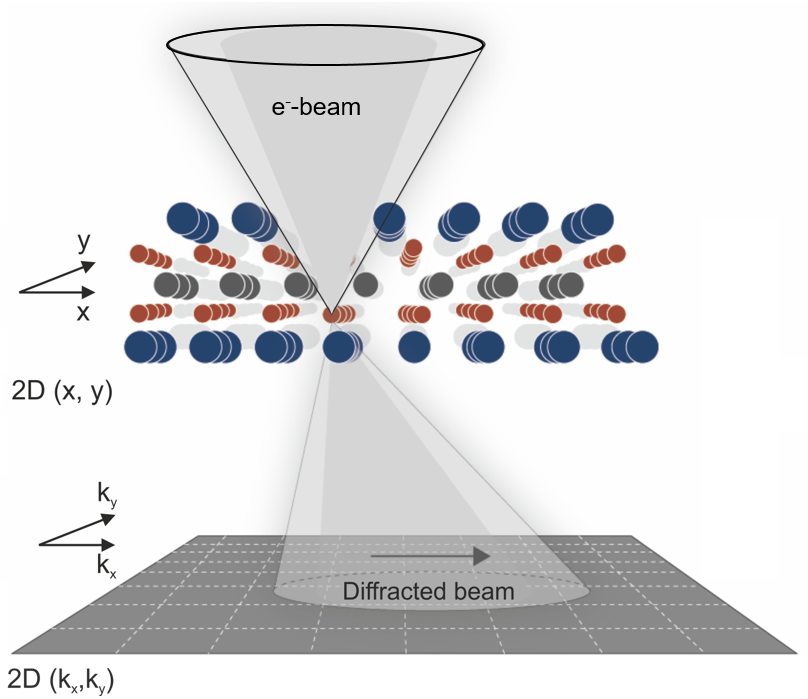
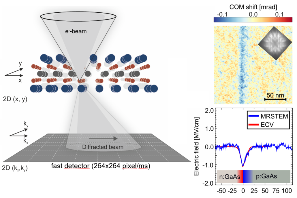
Nanometer-scale built-in electric field are the basis of many modern (opto)electronic devices, such as solar cells, lasers or batteries. Optimization of these devices requires precise characterization of such fields at small length scales. With a fast pixelated-detector, A. Beyer and coworkers in SFB project A5 (Volz) acquire a 2D diffraction pattern for every real-space position of the impinging electron beam. In doing so, the momentum transfer of an electric field (or a charge) on the electron beam can be measured, and the electric field, which is invisible in “normal high angle annular dark field images”, can be calculated from the 4D data-set.
In this work, key characteristics, like doping concentration or polarity, of GaAs-based p-n junctions were quantitatively obtained by 4D scanning transmission electron microscopy (4DSTEM). The values are in excellent quantitative agreement with results from other techniques, which – of course – lack lateral resolution.
Publication
A. Beyer, M.S. Munde, S. Firoozabadi, D. Heimes, T. Grieb, A. Rosenauer, K. Müller-Caspary, K. Volz
Quantitative Characterization of Nanometer-Scale Electric Fields via Momentum-Resolved STEM
Nano Lett. (2021) DOI:10.1021/acs.nanolett.0c04544
Contact
Prof. Dr. Kerstin Volz
Philipps-Universität Marburg
SFB 1083 project A5
Tel.: 06421 28 22297
EMAIL